Contact Us
For more information on our products or to contact USI directly, please complete the form:
Semiconductor
There are many scenarios where “nonstandard” semiconductor wafers and other flat substrates require the thin, uniform application of photoresist. Such cases include wafers with surface structures, features, or trenches, and wafers or substrates with non-circular shapes. The traditional spin coating method has proven ineffective in applying a thin, uniform coating in these cases and it wastes a significant amount of coating.
Other semiconductor applications include the deposition of polyimides, conductive inks and paints containing silver and copper, and liquids containing carbon nanotubes and nanoparticles.
Whatever the requirement, USI’s proprietary, nozzle-less ultra-Thin Coating Application Technology (tCAT) can provide the precision and reliability necessary.
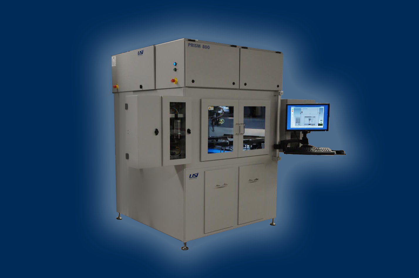
USI manufactures a full complement of high-performance spray coating equipment; the PRISM 400 BT Benchtop is designed for lab scale and R&D coating requirements, the PRISM-500 coating system is a small footprint, stand-alone tool suitable for low to mid volume manufacturing requirements and the PRISM-800 is engineered as a large format, high volume production machines.
Please visit our PRISM-400 BT (Benchtop), PRISM-500, and PRISM-800 product pages or contact us directly for more information.
USI Download Center
To download technical articles and product brochures, please click the following link:
USI Technical Library